

Highlights
Tiny device can detect hidden nuclear weapons, materials
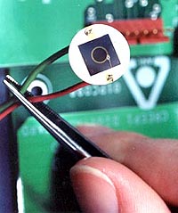
NUCLEAR DETECTOR -- This small wafer could become the key component in small, portable detectors for finding concealed nuclear weapons and materials. Argonne National Laboratory photo.
ARGONNE, Ill. (June 21, 2002) - A small, portable detector for finding concealed nuclear weapons and materials has been developed by the U.S. Department of Energy's Argonne National Laboratory.
When fully developed, the device could assist international inspectors charged with preventing smuggling and unauthorized use of nuclear weapons and materials.
The heart of the Argonne device is a small wafer of gallium arsenide (GaAs), a semiconducting material similar to silicon. When coated with boron or lithium, GaAs can detect neutrons, such as those emitted by the fissile materials that fuel nuclear weapons. Patents are pending on several detectors and their components.
The wafers are small, require less than 50 volts of power and operate at room temperature. They also can withstand relatively high radiation fields and do not degrade over time.
"The working portion of the wafer is about the diameter of a collar button, but thinner," said Raymond Klann, who leads the group from Argonne's Technology Development Division (now Nuclear Engineering Division) that developed the wafer and detector. "It is fairly straightforward to make full-sized detector systems the size of a deck of cards, or even smaller. Something that small can be used covertly, if necessary, by weapons inspectors to monitor nuclear facilities."
The key to detection, he said, is to coat the gallium-arsenide with something like boron or lithium. When neutrons strike the coating, they produce a cascade of charged particles that is easy to detect.
The wafers are made by co-inventor Doug McGregor at Kansas State University, who uses inexpensive, conventional microchip-processing techniques, Klann said. They can be tailor-made for specific applications by varying the type and thickness of the coating.
Compared to other neutron detectors, Klann's have a number of advantages.
One common type of neutron detector is based on a tube of gas, which is ionized when neutrons pass through the tube. These detectors are larger in size and require more power than the GaAs detector.
Another common neutron detector uses silicon semiconductors. Compared to the GaAs wafer, silicon-based detectors use more power, require cooling and degrade more quickly when exposed to radiation.
Klann's team also found that detection is improved by etching the wafer with cylindrical holes, like the dimples on a golf ball.
"We're testing various coating materials and thicknesses," he said, "as well as various combinations of hole sizes and spacings to find the best configurations for specific applications."
Klann's group has built and successfully demonstrated prototype detectors. Argonne is now looking for commercial partners interested in developing the detectors for the commercial marketplace.
Other possible uses for GaAs-based detectors include high-vacuum space applications or any other work requiring neutron detection.
Development of the wafer and detector was funded by the U.S. Department of Energy's Office of Science.
[ More News ]
Last Modified: Wed, April 20, 2016 9:33 AM